About
Overview
Leading full-spectrum financial services partner, driven by excellence

Leadership
Seasoned leaders spearheading our strategy, culture, and growth
Newsroom
The latest news and updates from the world of Avendus
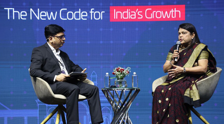
Events & Conferences
Flagship conferences and events with the industry’s finest
CSR
Driving change across communities for a sustainable, equitable future
Regulatory Information
Disclosures and policies guided by transparency
Leading full-spectrum financial services partner, driven by excellence
Seasoned leaders spearheading our strategy, culture, and growth
The latest news and updates from the world of Avendus
Flagship conferences and events with the industry’s finest
Driving change across communities for a sustainable, equitable future
Disclosures and policies guided by transparency

Insights
Expert perspectives, emerging trends, and in-depth sector analysis
Businesses
Investment Banking
Fuelling your boldest vision with seamless capital
Private Equity | Mergers & Acquisitions | Equity Capital Markets
Institutional Equities
Decoding markets to turn insights into opportunity
Wealth Management
Designing your wealth journey to build a lasting legacy
Asset Management
Delivering investment strategies aligned to your goals
Credit Solutions
Powering progress through tailored capital solutions
Fuelling your boldest vision with seamless capital
Private Equity | Mergers & Acquisitions | Equity Capital Markets
Decoding markets to turn insights into opportunity
Designing your wealth journey to build a lasting legacy
Delivering investment strategies aligned to your goals
Powering progress through tailored capital solutions
We Work With
Private Equity Strategies
Private Credit Strategies
Public Market Strategies
Careers
Overview
Build your career in a place where ambition and ownership thrive
Life at Avendus
A culture of excellence, integrity, and continuous learning
Why Avendus
Grow with curious minds, strong mentors, and meaningful work
Build your career in a place where ambition and ownership thrive
A culture of excellence, integrity, and continuous learning
Grow with curious minds, strong mentors, and meaningful work